 返回 高速大面积共聚焦拉曼... 返回 高速大面积共聚焦拉曼...
高速大面积共聚焦拉曼成像系统
超高性价比共焦拉曼成像系统!
高分辨率!
出色的重复性!
使用全息透射光栅,光透过率高!
可扩展/ 定制!
200µm x 200µm 图像快速扫描 & 2D Mapping!
韩国NANOBASE公司专业生产高性价比共聚焦拉曼成像系统,为科学和工业领域提供zei高性价比解决方案。新用户可以从购买基础款的XperRam Compact型拉曼光谱仪开始,之后可以通过不同的选项对拉曼光谱仪进行升级,以满足用户的不同需求。本产品具有超高性价,目前特惠价40万人民币,包含一套完整的激光拉曼扫描成像系统,同时可用于荧光,光电流成像
共焦拉曼成像系统,共聚焦拉曼成像系统,共焦拉曼光谱成像系统,共焦拉曼成像光谱仪系统,拉曼光谱仪,成像光谱仪,激光拉曼成像系统, 显微拉曼成像系统
韩国NANOBASE公司专业生产共聚焦激光扫描拉曼成像系统,为科学和工业领域提供zei高性价比解决方案。产品具有如下特点:
u 独特的激光扫描技术,具有优异的扫描分辨率和重复性
激光扫描分辨率< 0.02 um & 重复性< 0.1 μm
u 体相全息光栅光谱仪
光透过率>90%,比反射式光栅高30%,信号传输效率更高
u 具有Raman/PL/光电流等多种测量模式
u 结构紧凑,模块化设计
u 扫描速度快,扫描范围大
200µm x 200µm范围内高速成像 & 2D Mapping (x 40 objective)
产品参数:
上表是XperRam Compact与某知名公司拉曼光谱仪参数对比
u 光电流成像,大(重)样品测试
扫描成像,载物台无需移动,故而可以放置很重的样品在载物台上,下图是测量带制冷器的碳纳米管的光电流成像,普通拉曼成像系统无法完成此项测试

u 拉曼成像(二硫化钼)
 |
图(a)样品台上放置的带制冷器的碳纳米管的显微图像
 |
图(b)碳纳米管的光电流mapping图样,
设置为激光扫描区域180um x180µm,步2µm
可任意设置激光扫描范围和扫描步进,激光扫描范围在40倍物镜下zei大可达200µm x 200µm,激光扫描步进可低至0.1µm


图(c)二硫化钼样品的显微图像
图(d)二硫化钼的强度mapping成像,设置为激光扫描区域50um x50µm,激光扫描步进 0.3µm
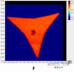
图(e)二硫化钼的强度mapping成像,设置为激光扫描区域30um x30µm,激光扫描步进 0.1µm
图(f)二硫化钼的频率mapping成像,设置为激光扫描区域30um x30µm,激光扫描步进 0.1µm
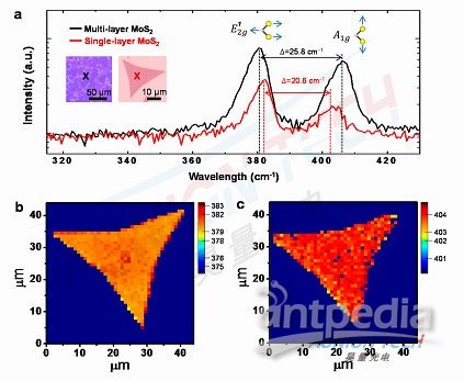
图(g)单层与多层二硫化钼薄膜拉曼成像与拉曼峰频移
u 荧光PL成像:

使用Nanobase XperRam系列拉曼成像光谱仪发表的部分文献:
(1) A Van Der Waals Homojunction: Ideal p–n Diode Behavior in MoSe2.pdf- Advanced Materials
(2) SemiconductorInsulator Semiconductor Diode Consisting of Monolayer MoS2, h‑BN, and GaN Heterostructure.pdf–ACS Nano
摘要:We propose a semiconductorinsulatorsemiconductor (SIS) heterojunction diode consisting of monolayer (1-L) MoS2, hexagonal boron nitride (h-BN), and epitaxial p-GaN that can be applied to high-performance nanoscale optoelectronics. The layered materials of 1-L MoS2 and h-BN, grown by chemical vapor deposition, were vertically stacked by a wet-transfer method on a p-GaN layer. The final structure was verified by confocal photoluminescence and Raman spectroscopy. Currentvoltage (IV) measurements were conducted to compare the device performance with that of a more classical pn structure. In both structures (the pn and SIS heterojunction diode), clear current-rectifying characteristics were observed. In particular, a current and threshold voltage were obtained for the SIS structure that was higher compared to that of the pn structure. This indicated that tunneling is the predominant carrier transport mechanism. In addition, the photoresponse of the SIS structure induced by the illumination of visible light was observed by photocurrent measurements.
更多资料详情请参见昊量
相关产品


 参考成交价格: